A cutting-edge simulation technique that combines artificial intelligence with traditional first-principles calculations has revolutionized the understanding of semiconductor circuit polishing mechanisms. This new Neural Network Potential (NNP) technology offers remarkable speed enhancements while maintaining the accuracy of first-principles calculations. By implementing NNP in the simulation of CMP slurry for semiconductor circuit polishing, Resonac has paved the way for rapid material discovery in the complex semiconductor manufacturing process.
In recent times, the semiconductor industry has been witnessing accelerated technological advancements, necessitating the swift delivery of new materials. Simulation techniques have been instrumental in expediting research and development for new materials. However, the semiconductor manufacturing process requires calculations of interactions at interfaces between materials with varying properties, posing challenges for traditional methods. NNP technology, with its ability to perform complex chemical reaction simulations at unparalleled speeds, offers a breakthrough in this regard.
Resonac’s introduction of state-of-the-art NNP technology in simulating the semiconductor substrate polishing process has allowed for a detailed understanding of intricate polishing mechanisms at the nanoscale level, leading to enhanced material discovery and shortened development timelines.
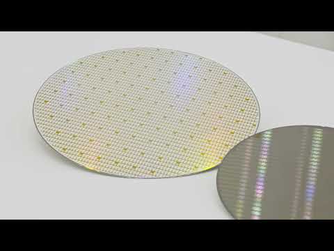
By simulating the polishing of silicon wafers using CMP slurry, intricate details of the process affected by surrounding environmental factors have been unveiled. This comprehensive understanding enables the identification of optimal raw material candidates to achieve high precision and desired functionality in new materials development.
NNP technology’s effectiveness in analyzing complex interfaces and heterogeneous mixtures extends beyond CMP slurry, making it a versatile tool for various semiconductor material applications.
Resonac’s pioneering utilization of NNP technology signifies a transformative era in material analysis and the discovery of innovative materials. The integration of AI semiconductor technologies has significantly elevated the performance of simulations, driving advancements in AI semiconductor development.
For further information on Resonac Group and its groundbreaking initiatives in the semiconductor and electron materials sector, visit their official website.
Exploring the Future of Semiconductor Polishing Through Innovative Simulation Techniques
In the realm of semiconductor manufacturing, the integration of cutting-edge simulation techniques has opened up new avenues for revolutionizing the polishing process. Building upon the foundation of traditional first-principles calculations, the application of Neural Network Potential (NNP) technology has introduced a paradigm shift in the semiconductor industry’s material discovery landscape.
# Key Questions:
1. How does NNP technology enhance the semiconductor polishing process?
– NNP technology accelerates simulations, but what specific advantages does it offer in terms of precision and efficiency?
2. What are the challenges associated with implementing NNP technology in semiconductor manufacturing?
– Are there any controversies surrounding the adoption of advanced simulation techniques in traditional manufacturing processes?
3. What are the advantages and disadvantages of utilizing NNP technology in material discovery for semiconductors?
– How does NNP technology compare to conventional methods in terms of cost-effectiveness and reliability?
# Insights and Challenges:
The rapid pace of technological advancements in the semiconductor industry necessitates quicker material development cycles. While traditional methods struggle with the complexities of interface interactions, NNP technology stands out for its ability to tackle intricate chemical reactions swiftly.
Resonac’s incorporation of NNP technology in substrate polishing simulations has shed light on the nuanced mechanisms governing the process at a granular level. This enhanced understanding not only expedites material discovery but also streamlines the overall development timelines.
# Advantages and Disadvantages:
Advantages:
– Rapid simulations lead to accelerated material discovery.
– Detailed analysis of environmental factors for optimized material selection.
– Versatility in analyzing complex interfaces and mixtures for various semiconductor applications.
Disadvantages:
– Potential challenges in real-world implementation and calibration of NNP models.
– Initial investments in AI integration may be substantial for some semiconductor manufacturers.
In conclusion, the collaboration of AI technologies with semiconductor manufacturing processes through NNP simulations marks a transformative era in the industry. The synergy between innovative simulation techniques and traditional methodologies is paving the way for groundbreaking advancements in semiconductor material discovery.
For more insights into the forefront of semiconductor and electron materials research, visit the [Resonac Group](https://www.resonacgroup.com) website.